VHDL PCI Target in Linux
Must ReadAt the moment I've lost interest in this project. The main bulk of the code is in place and the system does work. But I've still got to iron out a few small bugs and implement some extras, such as cache line support. It's no great deal to get this finished, but I'm working on other stuff at the moment.
One of the fastest ways to move data to and from the PC is via the PCI bus. Infact, most high speed PC interfaces are actually connected to the PCI bus (i.e. network cards). However, the high speed and versatility of the PCI bus does come at the expense of increased complexity.
This page documents my progress in interfacing an FPGA to the PCI bus of my PC. Why use an FPGA? The 33MHz clock and the 32-bit databus (plus control signals) really narrow down the choice when it comes to hardware selection. And when you take into account the processing power required to operate on the PCI bus, you narrow the choice down even further. I choose an FPGA as it's fast, has loads of I/O, and (best of all) is parallel.
I've choosen to operate the FPGA from the Linux operating system. I have 2 reasons for using Linux:
1) It makes a change from Windows.
2) It doesn't require commercial (expensive) software to develop the device driver.
At the moment I have no specific use for this project. In the past I've always used the serial port to move data to and from the PC. Although the serial port has the advantage of being easy to use it also has the major disadvantge of being slow (and serial). So I decided to look at what's involved in using the PCI bus. Some of the applications I plan to use the project for in the future include robotics and data logging.
At this moment in time I have no specific use for the PCI bus so I have 2 design choices:
1) Design a complete PCI core with backend logic.
2) Design a complete PCI system, which uses all of the PCI features.
Out of the 2 choices the PCI core is probally the best, but I feel it would require too much unenessary work. Having to design a generic interface to the PCI core, which would work in all cases, would be quite time consuming. So I've opted for the second choice. The system I've designed uses all the features of the PCI, bus it only has a basic I/O interface. The simple I/O interface can easily be extended with extra control signals, which would make it suitable for specific projects. After all, any PCI system, not matter how complex, basically boils down to reading and writing DWORD's to and from the PCI bus. How these DWORD's are processed is application specific and does not involve the PCI system.
The following is an attempt at a requirements specification. This will change as the project progresses, but it should help to explain what's on this page and it also acts as a basic introduction.
Requirements Specification
The FPGA needs to interface with the PCI bus of a standard PC. It should be capable of acting as a slave during target operations and a master during DMA operations. The FPGA must be able to run at 33MHz without the need for extra wait states. Interrupts must be supported as should any required configuration space registers. The FPGA must perform all these operations without the need for additional hardware (e.g. dedicated purpose made PCI controllers). All target PCI commands should be supported as should complete error checking (e.g. parity and device selection timeout). All FPGA development is to be done in VHDL.
Input to the system is via 8 DIP switches and output is via 8 LED's. During a write operation (to the PCI device) the least signaficant byte of each DWORD recieved, during the data phase, is displayed on the LED's. And likewise, during a read operation (from the PCI device) each DWORD read is made up of the value on the 8 DIP switches. The read and write operations are used in I/O space, memory mapped space, and DMA transactions.
The project is to be used in the Linux operating system. This requires a user space application and a kernel space device driver. The device driver needs to provide an interface to all of the supported features of the system (e.g. DMA). Both the device driver and the application are to be written in C.
As the version number suggests this project is still in its very early stages. The main jist of the code is in place with support for both master and slave transactions. A basic (and I mean basic) device driver has been developed along with an even more basic (and I mean even more basic) application to operate it. The following bullet points show the current progress of the project. These bullet points will be put into a proper change log at some point in the future.
Parts Completed (NOTE: Only very limited testing has taken place.)
 Configuration Space Reads
Configuration Space Writes
Custom Registers
Memory Mapped Reads
Memory Mapped Writes
Full Speed DevSel Timing
BusMaster Support (DMA To Device)
BusMaster Support (DMA From Device)
Retry's
Termination's.
Latency (limited)
Interrupts
Basic Linux Device Driver (DMA, Interrupts and memory mapped support)
Very Basic Linux Application
Configuration Space Reads
Configuration Space Writes
Custom Registers
Memory Mapped Reads
Memory Mapped Writes
Full Speed DevSel Timing
BusMaster Support (DMA To Device)
BusMaster Support (DMA From Device)
Retry's
Termination's.
Latency (limited)
Interrupts
Basic Linux Device Driver (DMA, Interrupts and memory mapped support)
Very Basic Linux Application
Not Yet Complete
Parity Checking (code is ready)
Cache Lines (basically this is just a counter)
Memory Read Multiple (needs Cache Lines)
Memory Read Line (needs Cache Lines)
Memory Write and Invalidate (needs Cache Lines)
DevSel Timeout (another counter)
Meet PCI Timing Requirements
Advanced Device Driver
Advanced Linux Application
Testing
Generate Backend Logic? (maybe)
Create a decent webpage
Other stuff I can't remember
I/O Read (minor changes)
I/O Write (minor changes)
The 'Not Yet Complete' list may look long but each of the items requires very little work (with the exception of the backend logic). The unsupported PCI commands (read multiple, read line, etc) require suprisingly little work to implement. The main bulk of the logic required for these commands has already been implemented for the memory mapped commands. As soon as I add support for cache lines all of the commands should be fully supported.
My Hardware Setup
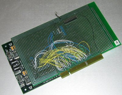
I've decided to describe my hardware setup as it may be of use to others who want to experiment with the PCI bus. The best setup would be to use a commercial FPGA PCI evaluation board and an expensive logic analyzer (or a PCI protocol analyzer). However, due to my limited budget a professional board and an expensive analyzer are unavailable to me.; Instead I'm using what I already have to hand, which happens to be a BurchED FPGA evaluation board and an 8-bit ANT-8 logic analyzer.
The BurchED evaluation board is not designed for PCI development, so it's not suprising to hear that it comes with no PCI connector. This problem is easily rectified by using a PCI road runner card. The type of FPGA used on the BurchED board is a Xilinx Spartan IIe, which uses 3.3V I/O. This introduces a problem as the PCI bus theoritacly runs at 5V. There are lots of ways to deal with the different levels, some of which are outlined in the following bullet points.
| Use dedicated QuickSwitches as recommended in a Xilinx Application Note (I can't remember which one). This is probally the best option, but I can't find any suppliers and they're all in a very small surface mount package. |
| Use some other level shifting IC. The PCI bus uses 33MHz bidirectional signals, which rules out all of the IC's I can find. |
| Use resistors. A Xilinx application note (I can't remember this one either) does say that the Spartan IIe is 5V tolerant if used with 100ohm series resistors. It also states that the output of the Spartan IIe is 5V TTL compatible. However, this does effect the rise and fall times of the signals. |
From the available level shifting options I have opted to use resistors. My main concern was the effect resistors would have on the rise and fall times of the PCI signals, but I've tried it and it seems to work. Although it should be noted that the use of resistors in this way most likely violates the strict timing requirements laid out by the PCI specification.
The interrupt signals of the PCI bus are a little different to other signals as they are tri-stated (pulled high rather than driven high). To deal with this I've used a MOSFET on each signal.
*****DIAGRAMDIAGRAMDIAGRAMDIAGRAMDIAGRAMDIAGRAMDIAGRAM
It's worth mentioning that although the PCI specification refers to 5V signalling, most modern motherboards only use 3.3V signals (this isn't the same as a 3.3V PCI bus). If your motherboard uses 3.3V signals you could probally (at your own risk) connect a 3.3V FPGA directly to the PCI bus. Something you have to take into account though is that any PCI cards connected to the motherboard can drive the PCI bus with potentially damaging 5V signals. These 5V signals may not show up during your initial measurements if the 5V PCI card is not in use. So even if your motherboard uses 3.3V signals I would strongly recommend the use of dedicated level shifting hardware.
Here's a picture of the BurchED board attached to the PCI road runner board.
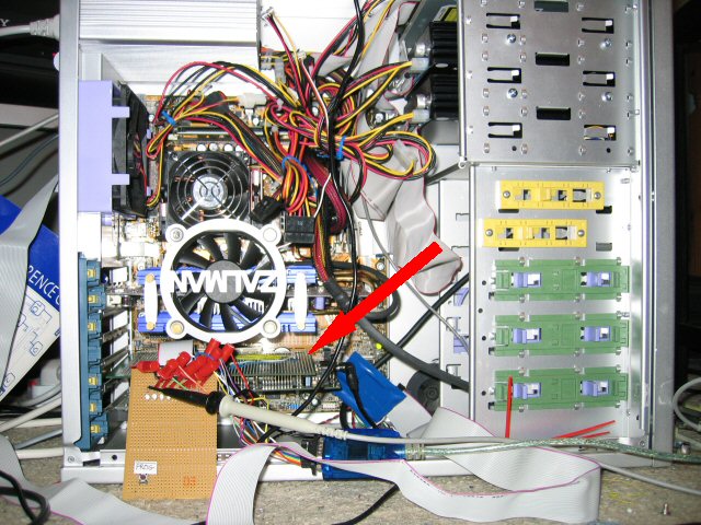
To make sure the card is working correctly I use 8 LED's. The LED's display the low byte of the data bus during data transfers to the card (MEM_WRITE and DMA_TODEVICE). I can also attach a logic analyzer to the LED's, which allows me to view the entire data transfer. Here's a picture of all the hardware in my PC.
Design Description
The Card in Linux
This section demonstrates the card working in Debian Linux. The VHDL code has been synthesised and then the FPGA has been programmed. The PC was then reset, which allows the BIOS to configure the (FPGA) PCI card up. These demonstrations were then performed.